
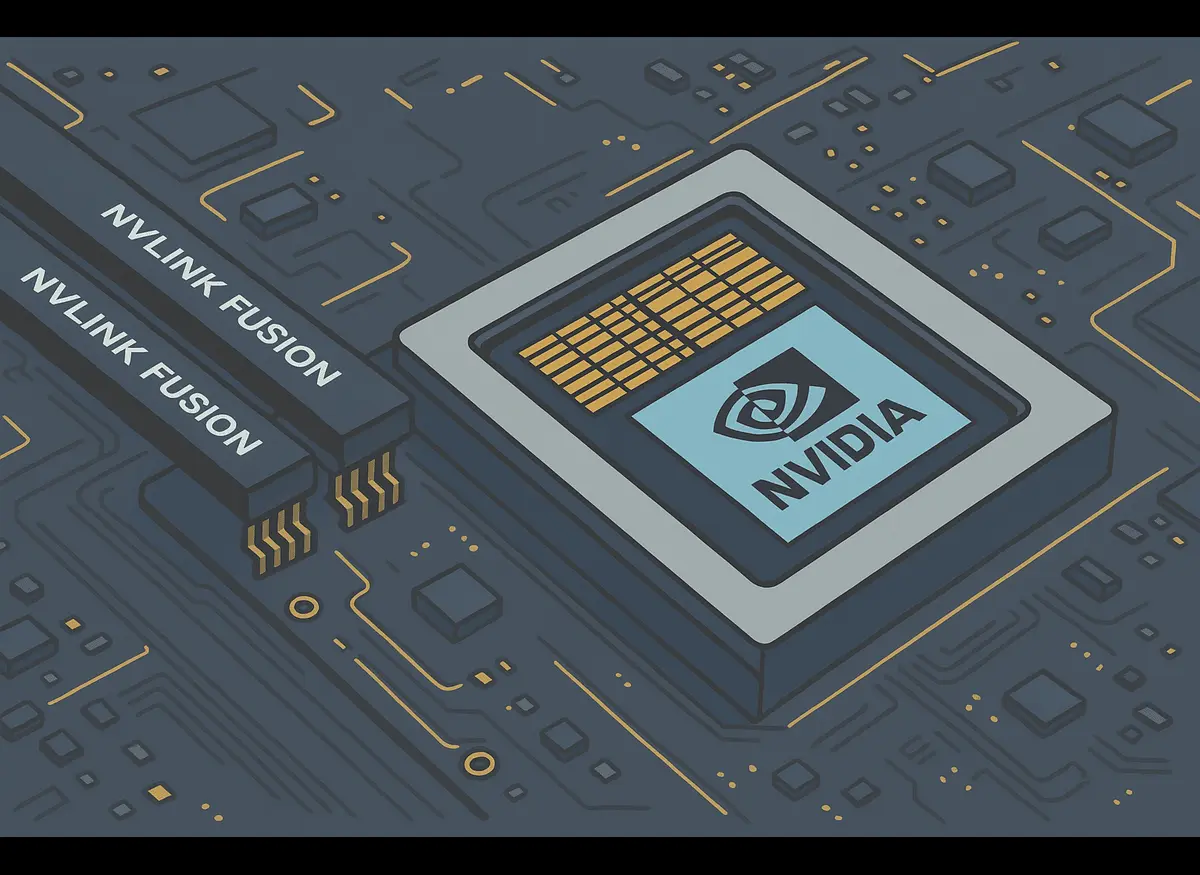
NVIDIA’s NVLink Fusion revolutionizes AI infrastructure with 1.8 TB/s bandwidth, 25x energy efficiency, and seamless GPU-CPU-accelerator integration. It enables scalable, high-performance AI systems while challenging open standards like UALink and redefining data center connectivity.
NVIDIA’s NVLink Fusion is set to redefine the very foundation of AI infrastructure by introducing a new standard in chip-to-chip connectivity. As artificial intelligence applications grow in scale and complexity, the need for ultra-fast, low-latency communication between processing units has become critical. NVLink Fusion addresses this demand with a transformative interconnect that combines unmatched bandwidth, energy efficiency, and system flexibility—positioning NVIDIA as a frontrunner in next-generation AI computing.
What Is NVLink Fusion?
NVLink Fusion is NVIDIA’s next-generation high-speed interconnect solution, designed to enable seamless communication across GPUs, CPUs, and custom accelerators. It introduces two major components:
- NVLink-C2C (Chip-to-Chip): A high-bandwidth, low-latency interface for direct inter-chip communication.
- NVLink 5 Chiplet: A modular silicon component that allows third-party accelerators to connect to NVIDIA’s architecture without accessing the full NVLink IP stack.
With 1.8 terabytes per second of bidirectional bandwidth, NVLink Fusion is 14 times faster than PCIe Gen5 and supports configurations of up to 72 accelerators in a single NVLink domain. This facilitates a non-blocking, all-to-all communication fabric, making it ideal for demanding AI workloads such as large language models (LLMs), generative AI, and real-time inference tasks.
NVLink Fusion vs PCIe Gen5: A Massive Leap Forward
Compared to PCIe Gen5, NVLink Fusion offers remarkable performance gains:
- 25x Greater Energy Efficiency: Reduces the power required for data transfer, lowering operational costs in data centers.
- 90x Better Area Efficiency: Optimizes silicon real estate, enabling more compact and powerful system designs.
- Lower Latency and Coherent Transfers: Ensures faster, synchronized communication between processing units.
These improvements make NVLink Fusion not just a faster alternative, but a fundamentally superior solution for next-generation AI systems.
Strategic Benefits for AI and Hyperscale Data Centers
NVLink Fusion is more than a hardware innovation—it is a strategic enabler for the AI revolution. Key advantages include:
Unmatched Performance at Scale
By delivering bandwidth far superior to traditional interconnects, NVLink Fusion allows enterprises to accelerate AI training and inference processes dramatically. This performance edge is crucial for businesses working with massive datasets and models, including transformers and multimodal systems.
Scalability for AI Factories
NVIDIA’s own GB300 NVL72 system, which uses NVLink Fusion, exemplifies the scalability it enables. With 72 NVIDIA Blackwell Ultra GPUs and 36 Grace CPUs, the system reaches 1.4 exaFLOPS of AI compute—providing the kind of infrastructure necessary for training frontier AI models.
Energy and Cost Efficiency
As data centers grapple with soaring power demands, energy-efficient technologies like NVLink Fusion are not just desirable—they’re essential. Reduced energy consumption translates directly into lower total cost of ownership (TCO), making the technology a wise investment for hyperscalers.
Flexible, Open Integration
Through NVLink-C2C and the NVLink 5 chiplet, NVIDIA offers an unprecedented level of architectural flexibility. Enterprises can integrate third-party CPUs and accelerators into standardized racks without compromising performance or coherence. This modularity streamlines both deployment and maintenance.
NVIDIA’s Expanding Ecosystem: A Calculated Growth Strategy
To broaden the adoption of NVLink Fusion, NVIDIA is partnering with industry leaders including MediaTek, Marvell, Qualcomm, Fujitsu, Alchip, Synopsys, and Cadence. These partnerships reflect NVIDIA’s strategic shift: opening its ecosystem while maintaining technological leadership.
At Computex 2025, NVIDIA announced that CPUs like Fujitsu’s Monaka and Qualcomm’s server-class chips will feature NVLink-C2C integration. The NVLink 5 chiplet, co-packaged with custom silicon, provides seamless compatibility with NVIDIA’s interconnect infrastructure—giving partners a plug-and-play gateway to high-speed communication.
Importantly, every deployment of NVLink Fusion still requires NVIDIA silicon (GPU or CPU), ensuring the company remains central to AI infrastructure while giving third parties controlled access to its ecosystem.
The Competitive Landscape: NVLink Fusion vs UALink and CXL
NVLink Fusion enters a competitive space currently being shaped by open standards like UALink (Ultra Accelerator Link) and CXL (Compute Express Link). Backed by companies such as Intel, AMD, and Broadcom, these standards promise interoperability and vendor neutrality.
However, NVLink Fusion offers significant advantages over its open-standard counterparts:
- Higher Bandwidth: UALink lags in throughput, making it less suitable for extremely high-performance applications.
- Chiplet Support: NVLink Fusion uniquely supports chiplet integration, enhancing modularity and design flexibility.
- Tight Ecosystem Optimization: NVIDIA’s end-to-end control over its architecture enables better optimization and reliability.
That said, some enterprises may still opt for open solutions to avoid potential vendor lock-in, especially in cost-sensitive markets.
Challenges and Considerations
While NVLink Fusion is a game-changing innovation, it is not without challenges:
- High Barrier to Entry: Integrating NVLink-C2C or using the NVLink 5 chiplet requires substantial investment and design expertise.
- Proprietary Model: Requiring NVIDIA hardware in every deployment may deter customers prioritizing open, interoperable solutions.
- Regulatory Concerns: As NVIDIA’s influence grows, antitrust scrutiny could emerge, similar to what other dominant tech players have faced.
- Partner Readiness: Smaller partners may face difficulties designing and validating custom silicon, despite the support offered by Synopsys and Cadence.
Overcoming these challenges will be key to NVLink Fusion’s long-term success.
Empowering the AI Revolution
Beyond its technical merits, NVLink Fusion helps unlock human potential. Whether it’s researchers modeling climate change, startups building language translation tools, or hospitals deploying real-time diagnostic systems, NVLink Fusion enables faster innovation.
By reducing communication bottlenecks and maximizing compute power, NVIDIA is helping to democratize access to high-performance AI—allowing more people to tackle the world’s toughest problems.
NVLink Fusion Sets a New Standard in AI Infrastructure
NVIDIA’s NVLink Fusion is more than an interconnect—it’s a bold vision for the future of AI infrastructure. With unparalleled bandwidth, energy efficiency, and integration flexibility, it positions NVIDIA as both a technology leader and a strategic partner for the world’s largest data centers.
As competition from open standards intensifies and regulatory eyes focus on tech consolidation, NVIDIA must continue balancing innovation with openness. But if the current trajectory holds, NVLink Fusion may well become the backbone of AI infrastructure for the next decade.In a world where speed, scale, and efficiency determine success, NVLink Fusion isn’t just the future—it’s already here.
Also read : Nvidia’s Computex 2025 Humanoid Robotics Breakthroughs: GR00T N1.5 and Beyond
AMD MI400 Chips & Helios Rack: The Future of AI Hardware in 2025
Discover more from Poniak Times
Subscribe to get the latest posts sent to your email.


